Tetragonal Trapezohedron Retrospective
I created the Tetragonal Trapezohedron LED polyhedron as part of the Idea 010 - Polyhedron Papercraft Mobile, and Idea 077 - Equilateral triangles LED panels projects.
This is the second polyhedron that I created in this series. The first was the dodecahedron, see the Dodecahedron PCB Retrospective for more information about the first.
This project expands on the Idea 077 - Equilateral triangles LED panels using a series of 8 uniform kite faced PCB boards instead of a equilateral triangle. Each face of the polyhedron has a grid of tiny LEDs arranged on the face, and mounting holes for a microcontroller on the back side. It is designed to be constructed into a 3D object where each panel’s edge is welded to the other to form a Tetragonal Trapezohedron polyhedron.
I have used this shape (Tetragonal Trapezohedron) before in my stained glass project (2019) Illuminated Stained Glass Tetragonal Trapezohedron that I showed at 2019 Vancouver Maker Faire.
The design files for this project and the previous shapes can be found on my Github project page PolyhedronMobile-PCB
This project cost about ~$100 USD shipped to my door via JLCPCB. 10 panels, with 2 spares. Components cost: $44.63, Shipping cost: $49.16, Customs duties & taxes: $6.70. Order Total: $100.49
What went right
It worked both electrically and mechanically
The board was simple enough that I wasn’t too worried about the electronics, it’s basically only LEDs and capacitors on the faces. Even if there were mistakes I left enough test points to be able to recover.
I was a little worried about the mechanical edges of the board and how I was going to be able to weld them together. My original idea didn’t work, but because I left mounting holes on the board I was able to fasten them together using wire.
Good size
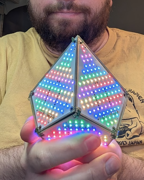
It’s about 200 mm high and 120 mm wide. About the size of a small eggplant. It fits nicely in cupped hands like a cupped ostrich egg.
The first Dodecahedron was a was about 30% larger and doesn’t fit in your hands. I am glad that I shrunk the size down.
Smaller and more LEDs
 On the first dodecahedron I only had 10x 5mm LEDs on each face. It worked but the resolution only allows me to make atmospheric colors without any patterns.
On this project I used much smaller 1.5mm LEDs XL-1615RGBC-WS2812B and tightly packed 101 LEDs per panel. 808 LEDs across the whole project. The tightly packed LEDs allow for much more complex patterns. It looks impressive with this many LEDs on it.
LED Layout
 I used a grind to lay out the LEDs. This made each panel symmetrical and ended up being visually appealing.
I was considering putting the LEDs in concentric circles or in a curve to add some complexity to the design but ended up going with the grid for simplicity. I am glad that I did.
Power consumption
I was worried that with so many LEDs it was going to consume too much power, and I would need to add power drops on every panel instead of one continuous power bus.
According to the datasheet XL-1615RGBC-WS2812B each LED consumes a maximum of 12mA at 5v.
12mA * 101 LEDs per panel * 8 panels = 9,696 mA @ 5v == ~48 Watts
48 Watts is a lot of power, especially if I wanted to run this off a USB power bank.
To compensate for this extreme power consumption, I configure the LEDs to use a max of 50% of their max brightness and create patterns that don’t use white often or illuminate all the LEDs at once.
A full white LED test consumed ~10 Watts (2,148 mA * 5v)
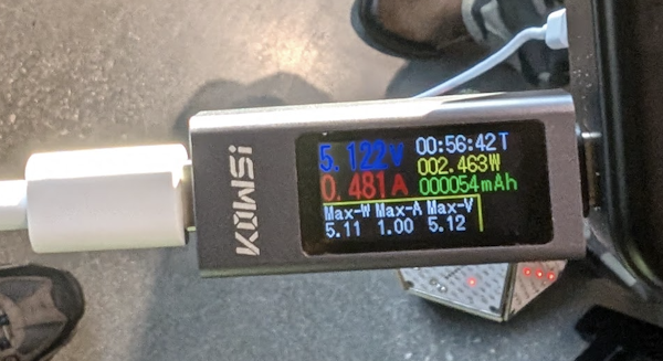
Under actual test of normal patterns it uses closer to 3 Watts (481mA * 5v). Well within the range of a normal USB-C power bank.
White PCB
I used white backed panels to help reflect the LED light. It gives it an elegant feel to it and works well. I plan to keep using white backed panels in the future.
Routing between each panel
I added in and out connectors to each panel. This allowed me to run wires between each panel instead of using the edge connections that I tried in the first version.
This allowed for a lot more flexibility, and creating the Hamiltonian path was much easier
What to change in the next version
Every iteration is a learning experience. I learned a lot in the Dodecahedron PCB Retrospective and was able to incorporate the lessons learned in this project.
I am hoping to figure out all the issues with this process in the less expensive shapes before moving on to the shapes that have 50+ panels.
Ground planes for the edge pads
 In the previous version I added corner connectors that I used to weld the panels together. This worked well and added enough strength to the shape to keep it together.
In this version I created a 2mm edge plate that wrapped the whole panel. The idea was that I could weld the panels together along the entire edge making them look more visually appealing than just the corners.
The problem was that I connected the edge plating to the ground plane in the boards. This means that if I wanted to weld the two edges together I would have to heat the entire ground plane of the panel hot enough that the solder would flow on to each panel. This is a lot of heat as the ground planes are huge and I would have to do that on both panels at the same time without desoldering the LEDs and other components on the panel.
It wasn’t possible and I made a few cold solder joins before giving up. The cold solder joins would come back to cause problems later on.
Because of this issue I moved on to trying to create a 3D printed sub structure to mount the panels to instead of using the edge platting to well everything together.
Leason learned
- Don’t connect pads to the grounding plane. This is why tools like KiCad add spokes to pads that are connected to the grounding plane to allow for welding.
Measurements in Fusion360 vs Inkscape vs KiCad
I originally designed the panels in Fusion360 to get the measurements correct. This allowed me to make 3D models of the shapes to ensure everything looked good and fit together.
Then I would export the panels as DFX files from Fusion360. The only file format that Fusion360 supports when exporting drawings.
I would take the DFX file and import it into Inkscape to clean up some of the geometry and remove duplicate lines, or construction lines from Fusion360. Saving the file as a SVG.
I would import the SVG into gingerbread to generate the KiCad geometry.
KiCad would eventually export the gerber files that would be sent to JLCPCB for manufacturing.
The issue was that Inkscape has terrible support for DFX. In general, Inkscape is terrible but it’s the goto free and open source tool for SVG editing so it’s used by many other tools built upon inkscape for editing SVG.
When the DFX is imported into Inkscape it skewes the dimensions ever so slightly. So small that I didn’t notice the issue when editing the files in Inkscape.
For example:
The height in Fusion360 and Inkscape is both 85.065mm as expected. While the height is 52.618mm in Inkscape and 52.573mm in fusion. A difference of 0.045mm.
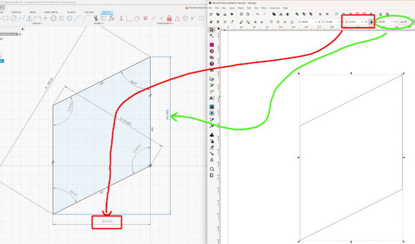
This isn’t an issue when mechanically fitting them together as the variants don’t add up enough to cause problems.
The issue comes into play when using the Fusion360 dimensions to design a 3D printed skeleton for the panels to be mounted to. That much of a difference causes the draft angle to be short and the panels don’t fit on top.
I redesigned the panels twice thinking my math was wrong, only to come to the same resulting models. I was feeling a lot of insecurities as this isn’t hard math, and yet I kept getting it wrong.
 Once I measured the physical panel using calipers and found that I was out by 1-2mm. I went through the process again and found out where the error came in. Fusion360 to Inkscape conversion.
Instead of redesigning the internal skeleton for the third time, I just tied the panels together using the mounting holes and some transparent fishing line.
Leason learned
- Never trust inkscape if you can avoid it
- Inkscape is not a CAD tool, its a drawing tool
Mechanical welding the edge pull traces near the edge
 After trying to weld the edges of the panels together and getting cold solder joins. I left the existing cold solder joins on the edges and tied the panels together using transparent fishing line.
While showing the project off at HackADay’s SuperCon 8, I dropped and squished the panels. Half of the project’s panels stopped working.
After I got home from the convention I took the project apart and found that when the two panels were squished, the cold solder joins on the edges pull the traces from the board ripping the data lines.
Leason learned
- Don’t put traces near the edge of the board
- Don’t connect the edge platting to the grounding plane or any traces
- Measure the physical panels instead of trusting the measurements in a CAD tool
Bad wireless connection
I am using a Seeed Studio Xiao ESP32-S3 as a micro-controller. It supports both bluetooth and Wifi, cheap, powerful, and tiny, and has built in lipo battery support.
On the inside of each panel I put a place to mount the micro-controller. I would populate only one panel with the micro-controller and leave the others unpopulated.
The idea was that I could control the patterns of the panels over wifi or bluetooth.
The issue was that because each panel is an electrical ground plane, the wireless signals couldn’t escape the inside of the object.
I ended up snaking the power and data lines out one of the grounding holes to an external controller that isn’t blocked.
Leason learned
- Wireless signals have a hard time escaping an enclosed grounded box.
- Don’t put the controller on the inside of the shape.
Battery only supplies 3.3 volts
The Seeed Studio Xiao ESP32-S3 micro-controller has pins and a charging controller for a Lipo battery.
My hope was to put a battery on the inside of the object that would power the LEDs for a short period of time. This would allow me to walk around with this object without being tethered to a power source.
The issue was that the micro-controller doesn’t have a boost converter built in. This means that the battery can at most provide 3.3v and when connected to the battery the 5v pin on the micro-controller only outputs 3.3v. 3.3v is not enough voltage to power the LEDs.
The Seeed Studio Xiao ESP32-S3 micro-controller’s data sheet mentions this, I just didn’t read it thoroughly enough.
This turned out to not be too much of a problem as I couldn’t put the micro-controller inside of the object because it would block the wireless signals anyways.
Leason learned
- Always read the datasheet
- battier powered projects are hard
- Investigate a 3.3 tolerant addressable LED
Power and data wiring and mounting options
 Since the micro-controller had to be removed from within the object, and the battery wasn’t going to be able to power the LEDs. I needed to run wires from within the object to the outside.
I had to snake the data and power calves out of one of the sets of mounting holes. This physically worked well as it also gave me a place to hang the object from.
The issue is that it looks appealing. I need to spend more time thinking about how to get power and data into the board. This might mean creating a specific hole for these cables. I need to think about how to do this in an appealing way as all the panels will have the same hole.
Throughhole
 The Seeed Studio Xiao ESP32-S3 micro-controller has castellated edge connectors that allow for the micro controller to be SMD welded to the panels.
When I created the footprint for the Seeed Studio Xiao board, I added both thought holes and SMD pads just in case I needed to attach some wires to other pins.
I didn’t end up needing the through holes, and every panel now has a series of holes that take away from the visual appeal of the panels.
In the next version, I won’t be placing the micro-controller inside and won’t need to have these holes.
Leason learned
- Spend more time thinking about the visual appeal of each panel. Don’t put “just in case” pads on the visible side of the panels.
Tiny pads for welding
 Each panel has a set of power and data pins. I use these pins to connect each panel to each other using some flexible wire.
I had the same problem that I had with the Dodecahedron where the default pads in KiCad for welding are too small. This makes it difficult to solder the connection wires.
I wanted to keep the connection in a standard 2.54mm spacing 01x03 connector. I needed to find a space for this connector between the grid of LEDs making it even harder to weld to afterwards. It would have been better if I separated these connectors and placed them in places that are easier to weld to.
Leason learned
- Make a custom footprint with larger pads to weld to
- Don’t restrict yourself to the 01x03 connector for the panel connections.
Two missing LEDs
 When laying out the LEDs on the panels, I tried to maximize the amount of LEDs that I placed without getting too close to the edge. For the most part it worked well but there was one place that I removed two LEDs that should be there.
I doubt most people would notice but I do.
Leason learned
- Print the board out so you can physically look at it and the spacing of all the components.
What’s next
Overall I am pretty happy with the way that this version worked out. I have a lot of changes to do in the next version.
For the next shape I am considering one of the following shapes.
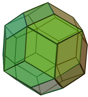
Rhombic triacontahedron - 30 panels is a lot of panels.
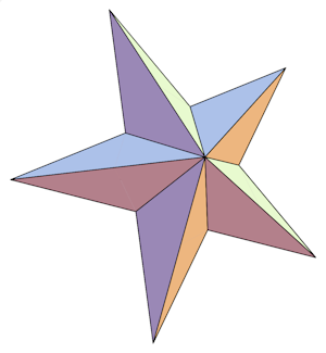
Pentagrammatic dipyramid - 20 panels and visually appealing but the math is harder.

Leave a comment