PCB Metro maps retrospective
The Idea 022 - Translink map PCB is part of the 100 Days of Ideas project from 2023.
The idea was to make a large PCB that was an interactive map of a metro train system. The plan was to embed an ESP32 into the PCB. Then write some software that would query the metro train API for real time train location. Then use this data to illuminate the stations when trains arrived.
I started with creating the Skytrain map for my home town Vancouver, BC. I went through several iterations of the design. I never felt that it was ever ready to be manufactured and it sat in my unfinished project folder for many months.
At the same time I was working on a project for the Washington DC Metro (WMATA) that was coming to completion. I had been working on this project for more than a year and I was looking to create a memento for this project. I also was looking to create some gifts for the people that helped with this project.
I decided that a PCB map of the Washington DC Metro (WMATA) would be a good memento and gift. I quickly designed the PCB in a few days and sent it to JLCPCB for manufacturing. I also decided to get the latest iteration of the Vancouver, BC Skytrain map manufactured at the same time, even though I wasn’t quite happy with the design.
The two boards came out very different from each other. I prefer the Washington, DC PCB Map over the Vancouver, BC, Skytrain PCB Map.
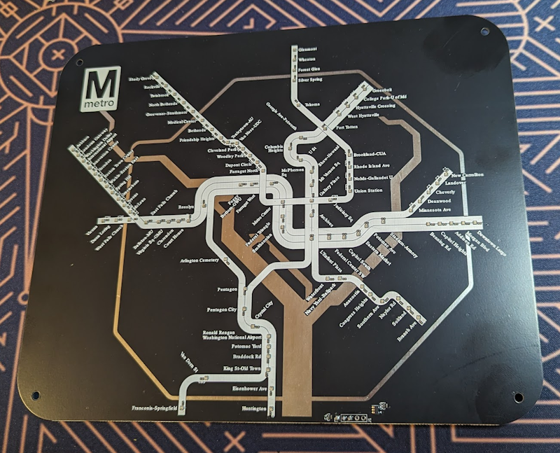
Washington, DC PCB Map
The Washington Metro PCB design files can be found on my Github.

What Went right
 I like that the black PCB solder masks make a good contrast with the white silk screen used for the train tracks. The silver exposed PCB traces that I used for the rivers and the ring road reflect well and are an interesting design element.
The simple WMATA logo in the top right helps reinforce that this is an infographic map of the metro train system. It’s a nice touch that a lot to the visual apples of the map
The LEDs illuminate off of the white silk screen for the train tracks and help create a more diffused look. They glow more than just a single point of light.
 The ring road made of exposed PDB traces really helped center the map well. It helped make the map look cohesive.
I installed WLED on the ESP32 to do test patterns for these boards. The “bouncing balls” pattern is quite attractive as a default.
I was worried that the station labels were going to be too small at 8 pt font but they look fine. They are legible and small enough that they don’t make the design too busy.
Overall I am pretty happy with this design.
What to change in the next version
I used the smallest LED that I could find on JLCPCB’s website. 1mm by 1mm WS2812B RGB LED.
I used these LEDs because they fit better on the small map within the train tracks. The map was already quite large. If I had to use the traditional 5mm by 5mm LEDs I would have needed to double the size of the map.
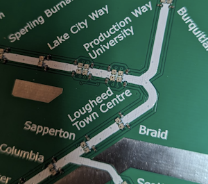
The issue was that 2 of the 5 boards had flaws in them related to these LEDs. They were just too damn small and flaked off of their solder pads. Rubbing my hands over one of the boards caused several LEDs to come loose. These LEDs are unreliable and I won’t use them again.
With the pads for the LEDs being so small I couldn’t try to resolder the LEDs to the board, and a hot air gun would have just blown the parts off immediately. The two boards with flaws were unrepairable.
Unlike the Vancouver BC PCB map, I didn’t add test points for each LED on the backside. This means that I could bypass the broken LEDs to get the rest of the map working. Design flaw.
 The PDB boards are 220 mm by 180 mm. I choose this dimension because it fits the map design well with no extra blank space. I wish I would have made it 230 mm by 230 mm so that It would have fit within the SANNAHED Ikea shadow box frame. This would have made mounting it or displaying the boards much easier. It’s so close to fitting in the box but the space at the top and bottom makes it look awkward. I think if I make another PCB map in the future I will design it with this frame in mind. Design flaw.
The capacitors next to each of the LEDs are no in a uniform orientation. Some of the capacitors are perpendicular to the LEDs, while others are parallel, and a few of them point off in a 45 degree angle. The orientation of the capacitors was placed to make sure that they fit within the silkscreen train tracks. More care could have been taken to make capacitor orientation uniform. It’s doubtful that anyone else will notice but I do. Design flaw.
 On the left side of the board on the Silver line, there are some capacitor component labels that I forgot to make invisible. They show up as C30, C31, etc… They aren’t too noticeable unless you know what you are looking for. Design flaw.
I should have doubled up the connector thougholes. Then I could have soldered wires to one set and test probes to the other set. This would have given me more options when mounting this board to the wall.
 The connector for the Data in, GND, and Power is too close to the edge of the board. I should have spaced it away from the edge more and off to the right hand side. It’s within 1mm of the edge making it hard to frame these PCBs because of the connector.
I should have added some unpopulated button pads on the back of the board to allow for some user configuration. A button to rotate through the different patterns, another to change the brightness of the LEDs. All the user options can be set via a web page but it’s nice to have physical buttons as an option.
L’Enfant Plaza, Metro Center, McPherson Sq station labels are confusing what LEDs are associated. There wasn’t a lot of room for these labels in the crowded center of the map. I am not sure what I could have done to make these better.
East Falls Church station label is pointing up to the right instead of down to the left. I did this to avoid overlapping with the ring road. It looks a little odd to be different then all the other stations in that section of the map. I had to overlap the ring road with labels of other stations, and I should have just done it here too.
I was thinking of adding the smithsonian mall, and the washington monument as icons on the map. They would have helped me better orientate myself on the map. Although it might make the map look too busy.
I spent a lot of effort ensuring that the PCB traces were behind the white silk screen. This was entirely unnecessary as the black solder mask entirely obscures the PCB traces. A lot of effort for no value.
Costs
- $19.90 Boards costs for 5 boards
- $70.81 Component costs for 5 boards
- $34.33 Shipping
- $23.70 Customs duties & taxes
$148.74 USD Total for 5 boards ($29.75 USD per board)
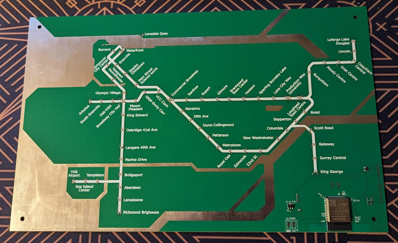
Vancouver, BC, Skytrain PCB Map
The Vancouver, BC, Skytrain PCB design files can be found on my Github.

What Went right
In general I am not too happy with this design.
What to change in the next version
3 of the 5 boards had the same flaws with the LEDs that the Washington Metro map had. I remembered to add test points to the back side of the board that allowed me to bypass the broken LEDs. This allowed me to salvage some of the broken boards.

In the Vancouver map I put two LEDs for each station. One for the incoming train and one for the outgoing train. Station hubs where two different lines meet I put four LEDs. Most of the LED flaws are on the stations where there are 4 LEDs next to each other.
The PCB map is huge, 300 mm by 190 mm. I could have easily reduced its size to 200mm wide without losing too much detail. The larger size makes it feel like there is a lot of empty unutilized space. It feels too empty.
Vancouver’s skytrain map is longer than its height. This makes it feel disproportionate in a way that the Washington DC map doesn’t with its ring road. I think shrinking the overall size of the map would have helped reduce this disproportionate feeling.
I used a green solder mask to represent the land of the map. It looks cheap with the green. While the black of the Washington DC map looks great. It’s very noticeable when the two maps are next to each other.
Just like the Washington DC map I used silver exposed PCB traces for the water. On the Vancouver map there is the Pacific Ocean and the Burrard Inlet and the Fraser river. That is a lot of water. Instead of the silvery color adding a nice highlight that catches the eye. All this water detracts from the rest of the map.
The silver exposed PCB traces that I used for the water are connected to the ground of the power supply. This means that it’s a giant grounding plane that if you touch it while touching a ground with a different potential it causes the LEDs to flicker. Design flaw
The silver exposed PCB traces that I used for the water show finger prints and oil.
 I embedded the ESP32 into the board. This seemed like a good idea when designing the board, but it added a lot of the cost of the boards without a lot of value. The Washington DC map has the ESP hot glued to the back of the board so that the front is nice and clean. Having the CPU separate from the board allows for more flexibility.
I didn’t round the corners of the PCB
I didn’t add the skytrain logo to the front of the board
Station labels are too large, I used a 12 pt font when I should have used an 8 pt font like the Washington DC map.
In general I am not too happy with this design.
Costs
- $26.50 Boards costs for 5 boards
- $107.13 Component costs for 5 boards
- $34.33 Shipping
- $23.70 Customs duties & taxes
$191.66 USD Total for 5 boards ($38.33 USD per board)

Leave a comment